TR220S DATASHEET
Version 1.2
Aug 26, 2026
Record History
| Version | Date | Detail |
| V1.0 | 2025-11-22 | First release |
| V1.1 | 2026-04-03 | Update description |
| V1.2 | 2026-08-26 | Update registers |
CONTENT
1.4.4. LCD INTERFACE PIN MAPPING
1.5.1. SPI INTERFACE(SPI-4WIRE, QSPI-4SDA)
1.6.4. PWM Duty Ratio Setting (20H)
1.6.5. PWM Frequency Setting (21H)
1.6.10. FONT Property Setting (75H)
1.6.11. 16*16 Standard FONT library(81H)
1.6.12. 24*24 Standard FONT library(82H)
1.6.13. CTP FUNCTION ENABLE (A0H)
1.6.16. Clearing TP STATUS(A3H)
1.6.17. RTP FUNCTION ENABLE(A4H)
1.6.20. Drawing RECTANGLE(B2H)
1.6.21. MIRROR AND ROTATION(ADH)
1.7. ELECTRICAL CHARACTERISTICS
DECLARATION
THIS DOCUMENTATION IS THE ORIGINAL WORK AND COPYRIGHTED PROPERTY OF Shanghai Top Display Optoelectronics (“TDO”). REPRODUCTION IN WHOLE OR INPART MUST OBTAIN THE WRITTEN APPROVAL OF TDO AND GIVE CLEAR ACKNOWLEDGEMENT TO THE COPYRIGHT OWNER.
THE INFORMATION FURNISHED BY TDO IS BELIEVED TO BE ACCURATE AND RELIABLE. TDO RESERVES THE RIGHT TO MAKE CHANGES IN CIRCUIT DESIGN AND/OR SPECIFICATIONS AT ANY TIME WITHOUT NOTICE. TDO DOES NOT ASSUME ANY RESPONSIBILITY AND LIABILITY FOR ITS USE. NOR FOR ANY INFRINGEMENTS OF PATENTS OR OTHER RIGHTS OF THE THIRD PARTIES WHICH MAY RESULT FROM ITS USE. NO LICENSE IS GRANTED BY IMPLICATION OR OTHERWISE UNDER ANY PATENT OR PATENT RIGHTS OF TDO. THIS DATASHEET NEITHER STATES NOR IMPLIES WARRANTY OF ANY KIND, INCLUDING FITNESS FOR ANY PARTICULAR APPLICATION.
THIRD PARTY LICENCES MAY BE REQUIRED TO IMPLEMENT THE SOLUTION/PRODUCT. CUSTOMERS SHALL BE SOLELY RESPONSIBLE TO OBTAIN ALL APPROPRIATELY REQUIRED THIRD PARTY LICENCES. TDO SHALL NOT BE LIABLE FOR ANY LICENCE FEEOR ROYALTY DUE IN RESPECT OF ANY REQUIRED THIRD PARTY LICENCE. TDO SHALL HAVE NO WARRANTY, INDEMNITY OR OTHER OBLIGATIONS WITH RESPECT TO MATTERS COVERED UNDER ANY REQUIRED THIRD PARTY LICENCE.
GENERAL SPECIFICATION
CPU
RISC-V 32bit,400MHz
With D-Cache and I-Cache
Embedded memory
PSRAM 4MB
Flash 2MB
Engine
DE (Display Engine):
One UI layer with 800x480@60Hz
GE (Graphic Engine):
Hardware rotation of 0, 90, 180, 270 degree
Hardware display mirroring
Hardware windowing
VE (Video Engine):
JPEG decoder with max.720P@60Hz
PNG decoder with max.720P@60Hz
Display Interface
Parallel RGB 16/18/24bits,Max. resolution 800x480@60Hz
DBU(Display Bridge Unit) input
Support 8080 8/16bit parallel protocol
Support 6800 8/16bit parallel protocol
Support 3/4-wire SPI、DSPI、QSPI protocol
8080/6800 8/16bit with max. 50MHz clock
3/4-wire SPI、4-SDA SPI with max.100MHz clock
Package
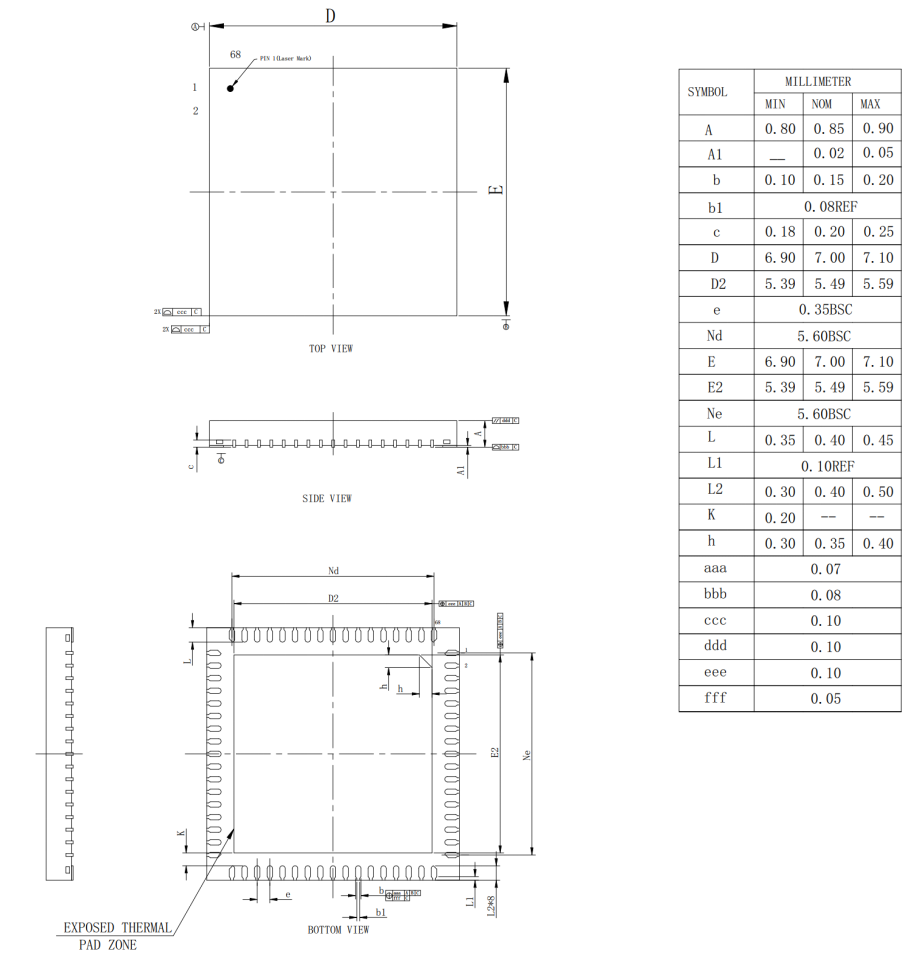
QFN68,7x7x0.85mm, pitch 0.35mm
Junction temperature
-20 ℃ to +105℃
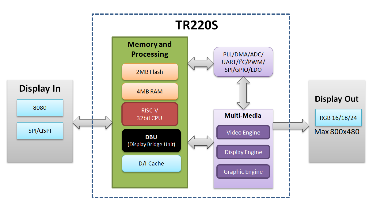
TR220S BLOCK DIAGRAM
DBU BLOCK
The DBU (Display Bridge Unit) module is tasked with receiving data from external MCUs and other peripheral systems. It captures image‑source signals, buffers them into RAM, and subsequently forwards the data to the DE for rendering and display. Within this application context, the external MCU acts as the host, while the TR220S operating via the DBU functions as the device. Functionally, TR230S is equivalent to a screen‑driver IC.
DBU Block Diagram:
PIN DEFINITION
DBU PIN
| Pin# | Symbol | Type | PIN Description | |
| 8080 | SPI /QSPI | |||
| 48 | PB8 | IO | WR#:WRITE strobe input | SPI-CLK /QSPI-CLK |
| 49 | PB9 | IO | RD#:READ strobe input | SPI-MOSI /QSPI-DATA0 |
| 50 | CS# | I | Chip selection, LOW active | |
| 51 | D/C# | I | DATA or COMMAND flag, D/C#="1": DATA or PARAMETER; D/C#="0": COMMAND | DATA or COMMAND flag, SPI-4WIRE interface needed: D/C#="1": DATA or PARAMETER; D/C#="0": COMMAND |
| 40 | PB0 | I | 8080-Data0 | |
| 41 | PB1 | IO | 8080-Data1 | |
| 42 | PB2 | IO | 8080-Data2 | |
| 43 | PB3 | IO | 8080-Data3 | |
| 44 | PB4 | I | 8080-Data4 | |
| 45 | PB5 | I | 8080-Data5 | |
| 46 | PB6 | I | 8080-Data6 | |
| 47 | PB7 | I | 8080-Data7 | |
| 66 | DBU_D8 | I | 8080-Data8 | |
| 67 | DBU_D9 | I | 8080-Data9 | SPI-MISO /QSPI-DATA1 |
| 68 | DBU_D10 | I | 8080-Data10 | QSPI-DATA2 |
| 1 | DBU_D11 | I | 8080-Data11 | QSPI-DATA3 |
| 2 | DBU_D12 | I | 8080-Data12 | |
| 3 | DBU_D13 | I | 8080-Data13 | |
| 4 | DBU_D14 | I | 8080-Data14 | |
| 5 | DBU_D15 | I | 8080-Data15 | |
| 6 | PD27 | O | LCD_DE | LCD_DE |
| 7 | PD26 | O | LCD_VS | LCD_VS |
| 8 | PD25 | O | LCD_HS | LCD_HS |
| 9 | PD24 | O | LCD_DCLK | LCD_DCLK |
| 10 | PD23 | O | LCD_D23 | LCD_D23 |
| 11 | PD22 | O | LCD_D22 | LCD_D22 |
| 13 | PD21 | O | LCD_D21 | LCD_D21 |
| 14 | PD20 | O | LCD_D20 | LCD_D20 |
| 15 | PD19 | O | LCD_D19 | LCD_D19 |
| 16 | PD18 | O | LCD_D18 | LCD_D18 |
| 17 | PD17 | O | LCD_D17 | LCD_D17 |
| 18 | PD16 | O | LCD_D16 | LCD_D16 |
| 19 | PD15 | O | LCD_D15 | LCD_D15 |
| 20 | PD14 | O | LCD_D14 | LCD_D14 |
| 21 | PD13 | O | LCD_D13 | LCD_D13 |
| 22 | PD12 | O | LCD_D12 | LCD_D12 |
| 23 | PD11 | O | LCD_D11 | LCD_D11 |
| 24 | PD10 | O | LCD_D10 | LCD_D10 |
| 25 | PD9 | O | LCD_D9 | LCD_D9 |
| 26 | PD8 | O | LCD_D8 | LCD_D8 |
| 30 | PD7 | O | LCD_D7 | LCD_D7 |
| 31 | PD6 | O | LCD_D6 | LCD_D6 |
| 32 | PD5 | O | LCD_D5 | LCD_D5 |
| 33 | PD4 | O | LCD_D4 | LCD_D4 |
| 34 | PD3 | O | LCD_D3 | LCD_D3 |
| 35 | PD2 | O | LCD_D2 | LCD_D2 |
| 36 | PD1 | O | LCD_D1 | LCD_D1 |
| 37 | PD0 | O | LCD_D0 | LCD_D0 |
POWER PIN
| Pin# | Symbol | Type | PIN Description |
| 12,29,54 | VCC33_IO | P | External 3.3V POWER supply input for IO |
| 27,53 | VDD11_SYS | O | Internal 1.xV LDO output, connect a 1uF decoupling cap.to GND for stabilization |
| 28 | LDO18 | O | Internal 1.8V LDO output, connect a 1uF and a 10uF cap.to GND for stabilization. Or supply an external 1.8V to this pin to reduce chip power dissipation. |
| 55 | LDO25 | O | Internal 2.5V LDO output, connect a 1uF decoupling cap.to GND for stabilization |
| 69 | GND | P | GND(It is also a thermal pad) |
OTHER GPIOs
| Pin# | Symbol | Type | PIN Description |
| 38 | BL-PWM | O | PWM output for controlling backlight driver |
| 39 | CTP-RST | IO | RESET for CTP,LOW active: Connecting to CTP-RST when driving CTP(Capacitive Touch Panel) by TR220S. |
| 52 | RESET# | I | RESET for TR220S and LCD. LOW active |
| 56 | DBG_TXD | IO | DBG_TXD:3.3VTTL UART_TRANSMIT,Reserving a test pad for updating F/W to TR220S, a 10Kohm pull-up resistor is needed |
| 57 | DBG_RXD | IO | DBG_RXD:3.3VTTL UART_RECEIVE, Reserving a test pad for updating F/W to TR220S,a 10Kohm pull-up resistor is needed |
| 58 | GPADC2 | IO | LCDInit-SPICLK: Connecting to panel when driving interface with RGB+SPI panel. CTP-SCL: Connecting to CTP-SCL when driving CTP(Capacitive Touch Panel) by TR220S(2.2K~4.7K pull-up needed). |
| 59 | GPADC3 | IO | LCDInit-SPIDATA: Connecting to panel when driving interface with RGB+SPI panel. CTP-SDA: Connecting to CTP-SDA when driving CTP(Capacitive Touch Panel) by TR220S(2.2K~4.7K pull-up needed). |
| 60 | GPADC4 | IO | LCDInit-CS: Chip select, connecting to panel when driving interface with RGB+SPI panel. |
| 61 | BUSY | O | BUSY STATUS flag, 0: Sending Command Not Allowed 1: Sending Command Allowed |
| 62 | RTP_YP | IO | RTP_YP: Connecting to Resistive touch Panel_YP if driving RTP by TR220S. IM0: INTERFACE CONFIGURATION PIN |
| 63 | RTP_XP | IO | RTP_XP: Connecting to Resistive touch Panel_XP if driving RTP by TR220S. IM1:INTERFACE CONFIGURATION PIN |
| 64 | RTP_XN | IO | RTP_XN: Connecting to Resistive touch Panel_XN if driving RTP by TR220S. Interruption FLAG: Connecting to user MCU when driving CTP(Capacitive Touch Panel) by TR220S; Not connecting when user driving CTP(Capacitive Touch Panel) via IIC directly. |
| 65 | RTP_YN | IO | RTP_YN: Connecting to Resistive touch Panel_YN if driving RTP by TR220S. CTP-INT: Connecting to CTP-INT when driving CTP(Capacitive Touch Panel) by TR220S. |
Notes: I=INPUT, O=OUTPUT, IO= INPUT AND OUTPUT, P=POWER
| PIN# | PIN Name | Mapping# | 0 | 1 | 2 | 3 | 4 |
| Bits/Pixel | 24 | 18 | 18 | 16 | 16 | ||
| Clks/Pixel | 1 | 1 | 1 | 1 | 1 | ||
| 37 | PD0 | LCD_D0 | B0 | NC | B2 | NC | B3 |
| 36 | PD1 | LCD_D1 | B1 | B3 | B4 | ||
| 35 | PD2 | LCD_D2 | B2 | B4 | B5 | ||
| 34 | PD3 | LCD_D3 | B3 | B5 | B6 | ||
| 33 | PD4 | LCD_D4 | B4 | B6 | B7 | ||
| 32 | PD5 | LCD_D5 | B5 | B7 | G2 | ||
| 31 | PD6 | LCD_D6 | B6 | B2 | G2 | G3 | |
| 30 | PD7 | LCD_D7 | B7 | B3 | G3 | G4 | |
| 26 | PD8 | LCD_D8 | G0 | B4 | G4 | B3 | G5 |
| 25 | PD9 | LCD_D9 | G1 | B5 | G5 | B4 | G6 |
| 24 | PD10 | LCD_D10 | G2 | B6 | G6 | B5 | G7 |
| 23 | PD11 | LCD_D11 | G3 | B7 | G7 | B6 | R3 |
| 22 | PD12 | LCD_D12 | G4 | G2 | R2 | B7 | R4 |
| 21 | PD13 | LCD_D13 | G5 | G3 | R3 | G2 | R5 |
| 20 | PD14 | LCD_D14 | G6 | G4 | R4 | G3 | R6 |
| 19 | PD15 | LCD_D15 | G7 | G5 | R5 | G4 | R7 |
| 18 | PD16 | LCD_D16 | R0 | G6 | R6 | G5 | NC |
| 17 | PD17 | LCD_D17 | R1 | G7 | R7 | G6 | |
| 16 | PD18 | LCD_D18 | R2 | R2 | NC | G7 | |
| 15 | PD19 | LCD_D19 | R3 | R3 | R3 | ||
| 14 | PD20 | LCD_D20 | R4 | R4 | R4 | ||
| 13 | PD21 | LCD_D21 | R5 | R5 | R5 | ||
| 11 | PD22 | LCD_D22 | R6 | R6 | R6 | ||
| 10 | PD23 | LCD_D23 | R7 | R7 | R7 | ||
| 9 | PD24 | LCD_DCLK | DCLK | DCLK | DCLK | DCLK | DCLK |
| 8 | PD25 | LCD_HS | HSYNC | HSYNC | HSYNC | HSYNC | HSYNC |
| 7 | PD26 | LCD_VS | VSYNC | VSYNC | VSYNC | VSYNC | VSYNC |
| 6 | PD27 | LCD_DE | DE | DE | DE | DE | DE |
LCD INTERFACE PIN MAPPING
Notes:
There are 5 MAPPING output configurations, the default is 24bits/Pixel, which can be configured to 18bits and 16bits, and the corresponding low bits are not used.
Mapping 0: Supports R/G/B signal interchange, and signal high-to-low sequence interchange within the group (Recommended using)
Mapping 1: Supports the exchange of the entire set of R/G/B signals (Recommended using)
Mapping 2: Supports R/G/B signal interchange
Mapping 3: Supports R/G/B signal interchange (Recommended using)
Mapping 4: Supports R/G/B signal interchange
INTERFACE DESCRIPTION
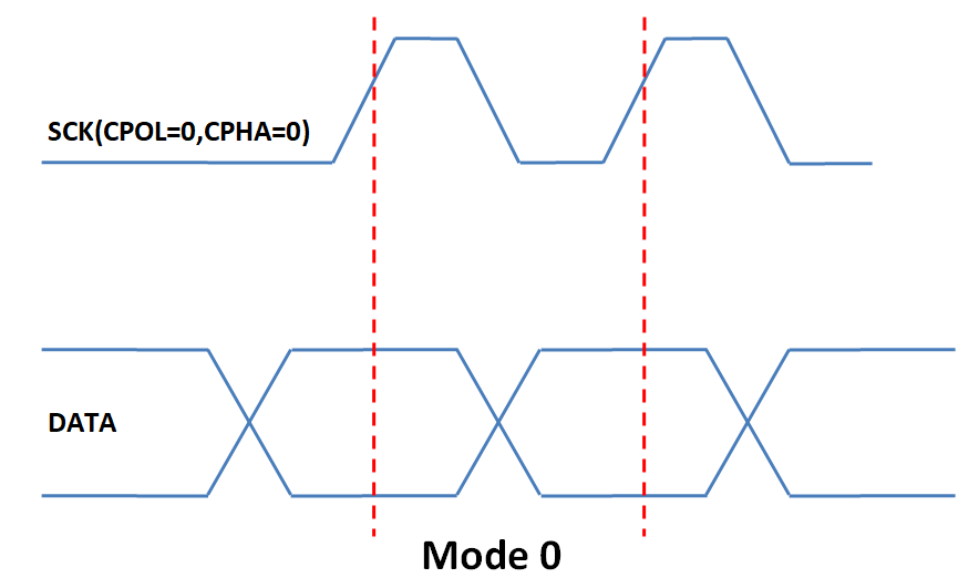
If there is no special indication, TR220S works on Mode0, that means data transmission occurs on the rising edge of the clock.
IM[1:0] Configuration table(6800 and DSPI is not commonly used and will not be described in this article):
| IMO | IM1 | INTERFACE | Related Pins | Max. Clock |
| 0 | 0 | SPI-4WIRE | CS#、SCL、SDO0、D/C#、BUSY | 100MHz |
| 1 | 0 | QSPI-4SDA | CS#、SCL、SDO0、SDO1、SDO2、SDO3、BUSY | 100MHz |
| 0 | 1 | 8080-8bit | CS#、D0~D7、D/C#、RD#、WR#、BUSY | 50MHz |
| 1 | 1 | 8080-16bit | CS#、D0~D15、D/C#、RD#、WR#、BUSY | 50MHz |
SPI INTERFACE(SPI-4WIRE, QSPI-4SDA)
PIN DESCRIPTION
| PIN NAME | Description |
| CS# | Chip selection: LOW active |
| SCL | Serial Interface Clock |
| SDO0 | SPI:MOSI QSPI: QSPI-DATA0 |
| SDO1 | SPI:MISO QSPI: QSPI-DATA1 |
| SDO2 | QSPI: QSPI-DATA2 |
| SDO3 | QSPI: QSPI-DATA3 |
| D/C# | DATA or COMMAND flag, 0:COMMAND 1:DATA |
| BUSY | BUSY STATUS flag, 0: Sending Command Not Allowed,1: Sending Command Allowed |
INTERFACE TIMING
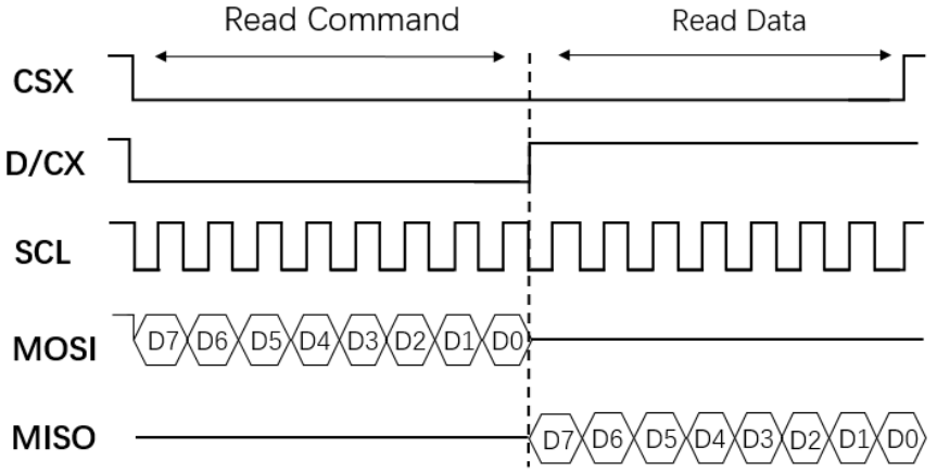
SPI-4WIRE
Timing for sending command and data:
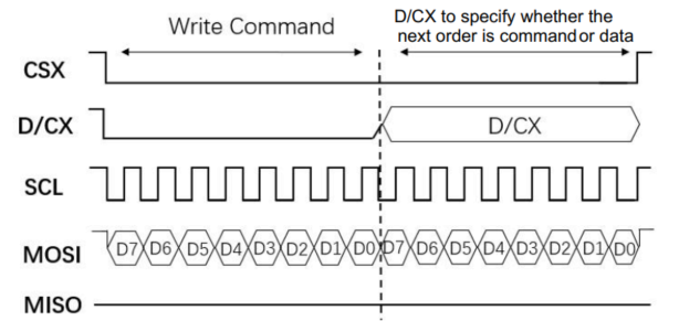
Timing for reading:
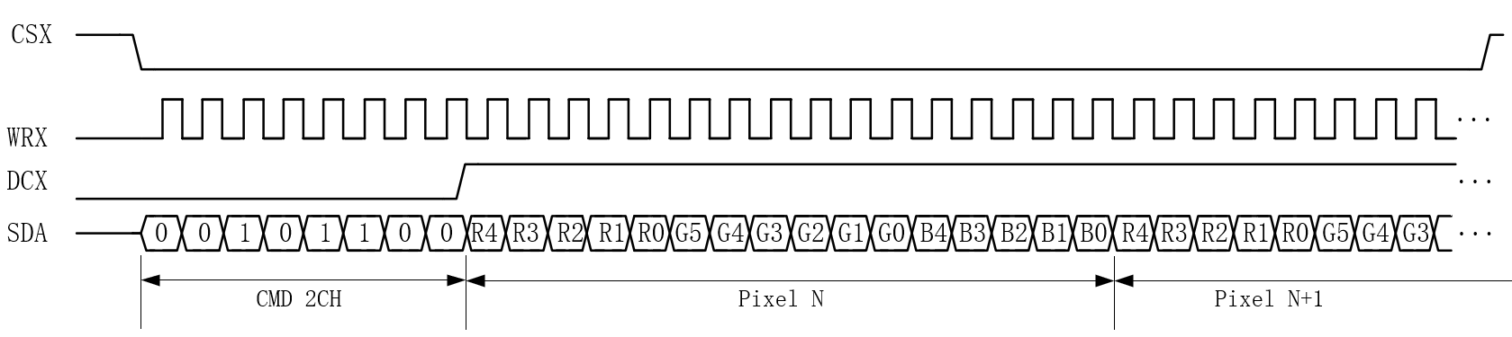
Display data writing format:
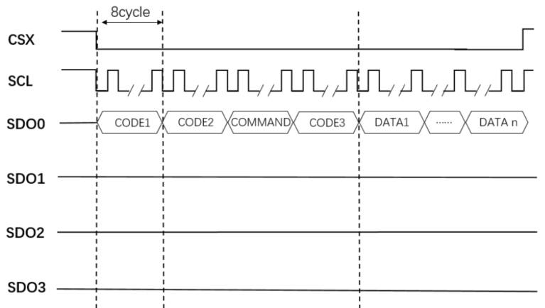
QSPI-4SDA
Timing for writing COMMAND and PARAMETERS:
(When CODE1=0x02, CODE2=CODE3=0x00)
Timing for reading:
(When CODE1=0x03, CODE2=CODE3=0x00)
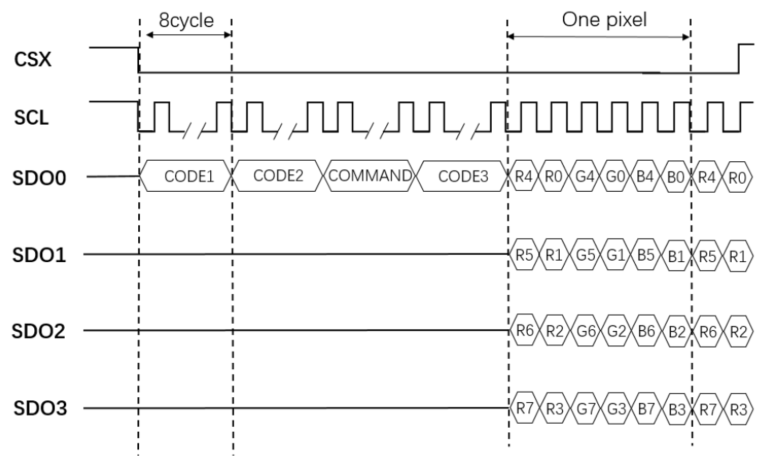
Display data writing format:
(CODE1=0x12, CODE2=CODE3=0x00 COMMAND = 0x2C)
8080 INTERFACE
PIN DESCRIPTION
| PIN NAME | Description |
| CS# | Chip selection: LOW active |
| WR | WRITE strobe input, rising edge effective |
| RD | Read strobe input, rising edge effective |
| DB0~DB15 | DATA BUS |
| D/C# | DATA or COMMAND flag, 0:COMMAND 1:DATA |
| BUSY | BUSY STATUS flag, 0: Sending Command Not Allowed 1: Sending Command Allowed |
INTERFACE TIMING (8080-8/16)
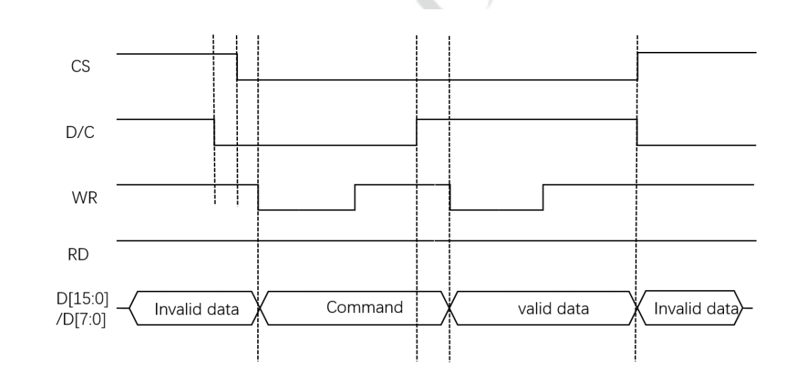
Timing for sending command and data:
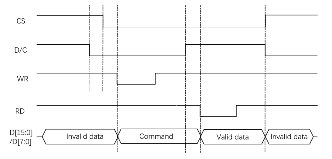
Timing for reading:
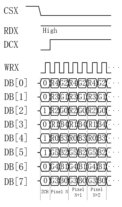
Display data writing format(8080-8B):
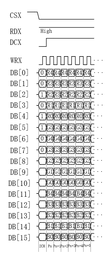
Display data writing format(8080-16B):
REGISTERs
Version(01H)
| Parameter | |||||||||
| W/R | D7 | D6 | D5 | D4 | D3 | D2 | D1 | D0 | |
| 1 Parameter | R | H | L | ||||||
| Description | Version: H.L | ||||||||
IC NAME(02H)
| Parameter | |||||||||
| W/R | D7 | D6 | D5 | D4 | D3 | D2 | D1 | D0 | |
| 1~8 Parameter | R | String | |||||||
| Description | IC: TR230S/TR220S | ||||||||
Self Test (12H)
| Parameter | ||||||||||
| W/R | D7 | D6 | D5 | D4 | D3 | D2 | D1 | D0 | Def | |
| 1 Parameter | W | format | 00H | |||||||
| Description | 0x00: Self test OFF; 0x01: Self test ON | |||||||||
PWM Duty Ratio Setting (20H)
| Parameter | ||||||||||
| W/R | D7 | D6 | D5 | D4 | D3 | D2 | D1 | D0 | Def | |
| 1 Parameter | W | Duty | 00H | |||||||
| Description | PWM duty ratio setting for backlight control: 0~100 (0x64 means 100% duty) | |||||||||
PWM Frequency Setting (21H)
| Parameter | ||||||||||
| W/R | D7 | D6 | D5 | D4 | D3 | D2 | D1 | D0 | Def | |
| 1 Parameter | W | CLK | 0AH | |||||||
| Description | PWM frequency setting for backlight control : 0~100KHz (0x64 means 100KHz) | |||||||||
COL_ADR (2AH)
| Parameter | ||||||||||
| W/R | D7 | D6 | D5 | D4 | D3 | D2 | D1 | D0 | Def | |
| 1 Parameter | W | X_S(H) | 00H | |||||||
| 2 Parameter | X_S(L) | 00H | ||||||||
| 3 Parameter | X_E(H) | 00H | ||||||||
| 4 Parameter | X_E(L) | 00H | ||||||||
| Description | Indicates the display size | |||||||||
ROW_ADR (2BH)
| Parameter | ||||||||||
| W/R | D7 | D6 | D5 | D4 | D3 | D2 | D1 | D0 | Def | |
| 1 Parameter | W | Y_S(H) | 00H | |||||||
| 2 Parameter | Y_S(L) | 00H | ||||||||
| 3 Parameter | Y_E(H) | 00H | ||||||||
| 4 Parameter | Y_E(L) | 00H | ||||||||
| Description | Indicates the display size | |||||||||
DISPALY DATA (2CH)
| Parameter | ||||||||||
| W/R | D7 | D6 | D5 | D4 | D3 | D2 | D1 | D0 | Def | |
| Display data | W | Display data | ||||||||
| Description | Display data push command(Special commands,Usage reference 1.5.1) | |||||||||
Soft Reset(5AH)
| Parameter | |||||||||
| W/R | D7 | D6 | D5 | D4 | D3 | D2 | D1 | D0 | |
| 1 Parameter | W | 0x01 | |||||||
| Description | Soft Reset | ||||||||
FONT Property Setting (75H)
| Parameter | |||||||||||
| W/R | D7 | D6 | D5 | D4 | D3 | D2 | D1 | D0 | Def | ||
| 1 Parameter | W | Kerning(H) | 00H | ||||||||
| 2 Parameter | Kerning(L) | 00H | |||||||||
| 3 Parameter | Space(H) | 00H | |||||||||
| 4 Parameter | Space(L) | 00H | |||||||||
| 5 Parameter | F_E | B_E | 00H | ||||||||
| 6 Parameter | F_COLOR(H) | 00H | |||||||||
| 7 Parameter | F_COLOR(L) | 00H | |||||||||
| 8 Parameter | B_COLOR(H) | FFH | |||||||||
| 9 Parameter | B_COLOR(L) | FFH | |||||||||
| Description | Kerning: Font spacing Space: Line spacing F_E: 0x0:Enable foreground color 0x1:Disable foreground color B_E: 0x0:Enablebackground color 0x1: Disable background color F_COLOR: Foreground color B_COLOR: Background color | ||||||||||
16*16 Standard FONT library(81H)
| Parameter | |||||||||
| W/R | D7 | D6 | D5 | D4 | D3 | D2 | D1 | D0 | |
| 1 Parameter | W | X(H) | |||||||
| 2 Parameter | X(L) | ||||||||
| 3 Parameter | Y(H) | ||||||||
| 4 Parameter | Y(L) | ||||||||
| 5~N Parameter | String | ||||||||
| Description | String: GBK character string with 16*16 dot matrix(ASCII characters displayed in a half width 8*16 dot matrix) | ||||||||
24*24 Standard FONT library(82H)
| Parameter | |||||||||
| W/R | D7 | D6 | D5 | D4 | D3 | D2 | D1 | D0 | |
| 1 Parameter | W | X(H) | |||||||
| 2 Parameter | X(L) | ||||||||
| 3 Parameter | Y(H) | ||||||||
| 4 Parameter | Y(L) | ||||||||
| 5~N Parameter | String | ||||||||
| Description | String: GBK character string with 24*24 dot matrix(ASCII characters displayed in a half width 12 * 24 dot matrix) | ||||||||
CTP FUNCTION ENABLE (A0H)
| Parameter | ||||||||||
| W/R | D7 | D6 | D5 | D4 | D3 | D2 | D1 | D0 | Def | |
| 1 Parameter | W | format | 00H | |||||||
| Description | 0x00: Disable touch function 0x01: Enable touch function | |||||||||
TP STATUS (A1H)
| Parameter | ||||||||||
| W/R | D7 | D6 | D5 | D4 | D3 | D2 | D1 | D0 | Def | |
| 1 Parameter | R | TP_STATUS | 00H | |||||||
| Description | 0x00: No touching events 0x02:Touching Releasing | |||||||||
TP Coordinate(A2H)
| Parameter | ||||||||||
| W/R | D7 | D6 | D5 | D4 | D3 | D2 | D1 | D0 | Def | |
| 1 Parameter | R | X(H) | 00H | |||||||
| 2 Parameter | X(L) | 00H | ||||||||
| 3 Parameter | Y(H) | 00H | ||||||||
| 4 Parameter | Y(L) | 00H | ||||||||
| Description | TP Coordinate (X,Y) | |||||||||
Clearing TP STATUS(A3H)
| Parameter | |||||||||
| W/R | D7 | D6 | D5 | D4 | D3 | D2 | D1 | D0 | |
| 1 Parameter | W | Format | |||||||
| Description | 0x00: To clear TP status | ||||||||
RTP FUNCTION ENABLE(A4H)
| Parameter | ||||||||||
| W/R | D7 | D6 | D5 | D4 | D3 | D2 | D1 | D0 | Def | |
| 1 Parameter | W | format | 00H | |||||||
| Description | 0x00: Disable touch function 0x01: Enable touch function | |||||||||
Drawing LINE(B0H)
| Parameter | |||||||||
| W/R | D7 | D6 | D5 | D4 | D3 | D2 | D1 | D0 | |
| 1 Parameter | W | X_S(H) | |||||||
| 2 Parameter | X_S(L) | ||||||||
| 3 Parameter | Y_S(H) | ||||||||
| 4 Parameter | Y_S(L) | ||||||||
| 5 Parameter | X_E(H) | ||||||||
| 6 Parameter | X_E(L) | ||||||||
| 7 Parameter | Y_E(H) | ||||||||
| 8 Parameter | Y_E(L) | ||||||||
| 9 Parameter | Width | ||||||||
| 10 Parameter | COLOR(H) | ||||||||
| 11 Parameter | COLOR(L) | ||||||||
| Description | Start(X_S,Y_S) End(X_E,Y_E) Width: Line width COLOR: Line color | ||||||||
Drawing CIRCLE (B1H)
| Parameter | |||||||||
| W/R | D7 | D6 | D5 | D4 | D3 | D2 | D1 | D0 | |
| 1 Parameter | W | X(H) | |||||||
| 2 Parameter | X(L) | ||||||||
| 3 Parameter | Y(H) | ||||||||
| 4 Parameter | Y(L) | ||||||||
| 5 Parameter | R(H) | ||||||||
| 6 Parameter | R(L) | ||||||||
| 7 Parameter | COLOR(H) | ||||||||
| 8 Parameter | COLOR(L) | ||||||||
| Description | Center of circle(X,Y) Radius(R) COLOR: Circle color | ||||||||
Drawing RECTANGLE(B2H)
| Parameter | |||||||||
| W/R | D7 | D6 | D5 | D4 | D3 | D2 | D1 | D0 | |
| 1 Parameter | W | X1(H) | |||||||
| 2 Parameter | X1(L) | ||||||||
| 3 Parameter | Y1(H) | ||||||||
| 4 Parameter | Y1(L) | ||||||||
| 5 Parameter | X2(H) | ||||||||
| 6 Parameter | X2(L) | ||||||||
| 7 Parameter | Y2(H) | ||||||||
| 8 Parameter | Y2(L) | ||||||||
| 9 Parameter | COLOR(H) | ||||||||
| 10 Parameter | COLOR(L) | ||||||||
| Description | Coordinate of the upper left corner of the rectangle (X1,Y1), Coordinate of the bottom right corner of the rectangle (X2,Y2) | ||||||||
MIRROR AND ROTATION(ADH)
| Parameter | ||||||||||
| W/R | D7 | D6 | D5 | D4 | D3 | D2 | D1 | D0 | Def | |
| 1 Parameter | W | format | 00H | |||||||
| Description | 0x00:No Rotation 0x01:Rotation 90° 0x02:Rotation 180° 0x03:Rotation 270° 0x10:X-axis mirror image 0x20:Y-axis mirror image | |||||||||
ELECTRICAL CHARACTERISTICS
Absolute Maximum Characteristics
| Description | Min | Max | Unit |
| Storage Temperature | -40 | 125 | °C |
| In/Out current for input and output | -50 | 60 | mA |
| I/O input voltage | -0.3 | 3.6 | V |
| Power Supply for VCC | -0.3 | 3.6 | V |
Recommended Operating Conditions
| Description |
|
| Max | Unit |
| Ambient Operating Temperature |
|
| 85 | °C |
| Junction Temperature |
| 105 | °C | |
| Power Supply |
|
| 3.6 | V |
I/O Characteristics
|
|
|
|
| Unit |
|
|
|
|
| V |
|
|
|
|
| V |
|
|
| KΩ | ||
|
|
| KΩ | ||
|
|
|
|
| uA |
|
|
|
|
| uA |
|
|
|
|
| V |
|
|
|
|
| V |
|
|
|
|
| uA |
|
| - | - |
|
|
|
| - | - |
|
|
PACKAGE